Contents
EMSim is the foundation laid in my Tianjin University Ph.D. thesis. The AI-acceleration extensions — EMSim+ (GAN, then GAN+TL) and AIPS — were led by Ya Gao, whose research I supervise, with me co-authoring. This post tells the lineage as one story.
Why pre-silicon evaluation?
Cryptographic integrated circuits sit at the core of every system that needs to establish trust. A bank card authenticates a transaction; an IoT sensor proves its identity to a gateway; a hardware security module (HSM) protects keys for a datacenter’s signing infrastructure. In each case, a dedicated IC runs algorithms like AES for symmetric encryption or Kyber for post-quantum key encapsulation, handling secrets that never leave the chip’s boundary — at least in principle.
Side-channel analysis (SCA) attacks that boundary without ever touching the algorithm itself. When a chip computes, it consumes power, radiates electromagnetic (EM) fields, and completes operations in time intervals that vary with the data being processed. None of those effects are intentional outputs, but all of them carry information correlated with the chip’s internal state, including the secret key. An attacker who can measure power traces, EM emanations, or timing differences from a running device can recover key material statistically — no vulnerability in the cipher’s mathematics required.
The statistical machinery is well established. Differential power analysis (DPA) and its generalization, correlation power analysis (CPA), compare measured traces against a model of what a chip that holds a candidate key byte ought to look like, scanning the key space until the correct hypothesis produces a peak. The non-specific t-test (TVLA) splits traces on a data-dependent criterion (e.g., fixed plaintext vs. random) and applies a t-test to check whether the two distributions differ — if they do, the device leaks. None of this requires solving a hard mathematical problem; it requires enough measurements and enough computation, both of which are cheap.
In practice, the attacker’s setup is modest: a digital oscilloscope, a current probe or EM near-field probe positioned over the chip package, and a workstation running open-source analysis tools. Recovering a 128-bit AES key may take a few thousand to a few hundred thousand power traces depending on the device’s countermeasures — a collection campaign that can run in hours on a benchtop. EM measurements can be even more localized, targeting small regions of the die without decapping.
The conventional response is to evaluate a chip after it comes back from the foundry, characterize its leakage, and redesign if the result is bad. That response is increasingly untenable. Taping out a chip at advanced process nodes costs tens of millions of dollars; at older nodes the figure is lower but still substantial. More critically, the design-to-silicon cycle runs months — simulation, layout, verification, tape-out, fabrication, packaging, bring-up. If the first silicon leaks, the team must iterate the full cycle while a launch date slips and a vulnerable product potentially sits in a shipping pipeline. Time-to-market pressure routinely turns “we’ll fix it in the next spin” into “we’ll add a software mitigation and ship.”
Pre-silicon evaluation changes the economics. The idea is to simulate the physical leakage — power consumption or EM emanations — directly from the chip’s design, before any silicon exists, so that countermeasures can be validated, vulnerabilities can be caught and fixed before tape-out, and the design team can arrive at tape-out with evidence that the chip is resistant. Edits at the RTL (register-transfer level) or layout stage cost engineering time, not foundry runs.
The simulation challenge
Pre-silicon SCA evaluation has two demands that must be satisfied simultaneously. First, the simulated leakage waveforms must be accurate enough that a statistical attack run against them produces the same verdict it would produce against real silicon — if the simulation says the design is leaky, there has to be an actual leakage mechanism to point at. Second, the trace counts must be large enough to actually run those attacks credibly: CPA and TVLA campaigns routinely need 100K–1M traces to achieve reliable key recovery or to rule out leakage with statistical confidence. Both demands run head-on into four concrete problems.
-
Physics-based EM simulation doesn’t scale to campaign-sized trace counts. Layout-level electromagnetic simulation is the rigorous starting point. It respects parasitic networks, metal-wire geometry, and the physical mechanisms that determine where and how a design radiates. But commercial EDA (electronic design automation) flows are built for design verification, not trace generation at scale: a physics-based EM simulation of a single power trace can take minutes. At that rate, generating 100K traces takes months on a workstation, or a compute budget that no design team can justify on a pre-tapeout evaluation.
-
Even accelerated physics simulation is still too slow for full campaigns. Speed improvements that bring single-trace simulation from minutes down to seconds help — but they don’t close the gap. Even a 32× speedup over the baseline still leaves a 100K-trace campaign needing days.
-
A learned simulator trained on one design doesn’t transfer to the next. Machine learning models for leakage simulation are trained on a specific chip’s layout, process parameters, and operating conditions. When a design changes — a different crypto core, a new countermeasure, a technology node migration — the model’s assumptions break down and it must be retrained from scratch. In a design iteration loop, that means paying the training cost at the moment it’s most disruptive: exactly when engineers need fast answers about whether a proposed fix closed a leakage path.
-
Power simulation for SCA is a different problem from what EDA tools solve today. Electromagnetic leakage is one attack channel; power is the most extensively studied one, and the channel most designers think about first because probe placement is simpler and the literature is deeper. But the simulation tools designers already use — waveform-accurate power analysis in flows like PrimeTime PX — are built to answer thermal and voltage-variation questions, where average power over a clock cycle is what matters. SCA attacks depend on the nanosecond-scale transient waveforms that encode data-dependent transitions in individual logic paths.
The next four sections take these four problems in order and describe what we did about each.
EMSim — physics, accelerated
Layout-level electromagnetic simulation is, in principle, the right answer to Problem 1. It starts from physical reality: the chip’s geometry as actually laid out, the parasitic capacitances and resistances of real metal wires, the switching currents that flow through every net on every clock edge. A simulation grounded at that level captures what RTL-level estimates cannot: the spatial structure that shapes what an EM probe actually measures. The problem is not correctness. The problem is cost.
Commercial EDA flows are built for design verification, not for trace generation at campaign scale. Running a physics-accurate EM simulation of a single power trace through a layout-parasitic extraction netlist can take several minutes on a workstation. That number does not sound alarming until you multiply it: 100,000 traces — a modest SCA evaluation campaign — would require months of compute time. A million traces, which leakage certification increasingly demands, pushes the estimate past any reasonable pre-tapeout budget.
EMSim was built to attack this throughput gap directly without abandoning the physics.
The starting point is understanding why EM emanation looks the way it does at layout level. When a chip switches logic states, time-varying currents flow through metal interconnects — particularly the top-layer power and ground straps that distribute supply voltage across the die, and the clock tree that fans out through the hierarchy beneath them. Those currents produce magnetic fields whose spatial and temporal pattern is what a near-field EM probe samples. Layout geometry is what determines the field: the wire lengths, their orientations, their distances from the probe, and the currents they carry at each moment in time. Two chips implementing the same RTL in different floorplans will produce measurably different EM signatures. Simulation that does not account for layout geometry cannot predict what an attacker will measure.
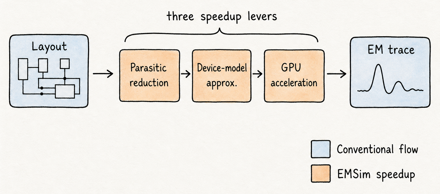
EMSim’s speedup comes from three levers applied in sequence, each targeting a different bottleneck in the simulation pipeline.
Parasitic-network reduction addresses the first bottleneck: the extracted parasitic netlist for even a modest block can contain millions of RC nodes, most of which have negligible effect on the integrated current waveforms that drive EM emanation. EMSim identifies and collapses sub-threshold parasitics — nodes whose contribution to the relevant EM-driving currents falls below a calibrated threshold — without materially changing the field prediction. The reduced network retains the nodes that matter while discarding the ones that exist only for thermal or voltage-drop analysis purposes.
Device-model approximation addresses the second bottleneck: SPICE-grade transistor models were designed to support sub-threshold accuracy, quasi-static analysis, and precise voltage-settling — fidelity that is expensive to compute and largely irrelevant for EM prediction. What EM simulation needs is not quasi-static accuracy but integrated-charge accuracy: how much charge moved through a net, and when. EMSim replaces full transistor models with simplified dynamic-current approximations tuned to match the integrated-charge behavior of the full model at a fraction of the evaluation cost.
GPU acceleration addresses the third bottleneck. After parasitic reduction and model approximation, the simulation problem is a large, sparse linear system that must be solved for each time step of each trace. Those systems are not small, but they are parallel-friendly: the structure that makes them hard to solve serially on a CPU makes them well suited to the thousands of parallel arithmetic units on a modern GPU. Moving the solver to GPU reduces per-trace wall-clock time from minutes to seconds.
The interaction of layout geometry and current waveforms that drives all three levers can be made precise. The magnetic field at a sensor location r produced by the chip’s metal interconnect is:
\[\mathbf{B}(\mathbf{r}, t) \;=\; \frac{\mu_0}{4\pi} \sum_{w} \int_{\ell_w} \frac{I_w(t)\,d\boldsymbol{\ell} \times (\mathbf{r} - \mathbf{r}')}{\|\mathbf{r} - \mathbf{r}'\|^3}\]Read this as: the magnetic field at any sensor point r is a geometry-weighted sum of contributions from every wire’s current. Two implications follow immediately. First, layout determines the EM signature — RTL alone cannot tell you what an attacker will measure, because the geometric factor in the integral is a function of wire position and orientation, not logic function. Second, accurate EM simulation requires accurate per-wire current waveforms, which is exactly what EMSim’s three levers are working to produce efficiently: reduce the network to cut solver cost, approximate the device models to cut per-step evaluation cost, and move to GPU to exploit the parallelism that remains.
EMSim was validated on S-Box and AES designs fabricated in SMIC 180 nm. EMSim’s intrinsic accuracy — the normalized cross-correlation between simulated and silicon signals — reached 74% in the time domain and 98% in the spatial domain (across probe positions). Attack prediction accuracy reached 93%: when EMSim flagged a design as leaky, silicon agreed 93% of the time. The overall simulation speedup over the baseline EDA flow was 32×, bringing individual trace generation from minutes into the seconds range.
EMSim+ (GAN) — learning to simulate
Thirty-two times faster is a real gain. It is not enough. The benchmark for credible SCA evaluation — a full CPA or TVLA campaign at sufficient statistical power to either recover a key or certify the absence of leakage — sits in the range of 100K to 1M traces. EMSim brings per-trace cost from several minutes into the seconds range, but seconds-per-trace × millions of traces is still on the order of weeks of compute time. That arithmetic does not fit a design iteration loop. The physics-based speedup moved the wall; it did not remove it.
The next order of magnitude cannot come from further tuning the same physics pipeline. Parasitic reduction, device-model approximation, and GPU parallelism have already harvested the tractable gains. What the problem needs is a different shape of computation entirely — one where the expensive work is paid once, and individual traces after that cost nearly nothing.
The key observation is that the physics simulator, slow as it is, is a function: given a description of what is happening in the chip at a moment in time — which cells are switching, how much current each is drawing, how that current distributes through the power grid and clock tree — EMSim returns the EM map at the chip surface. That function is deterministic and smooth over its inputs. It can, in principle, be learned.
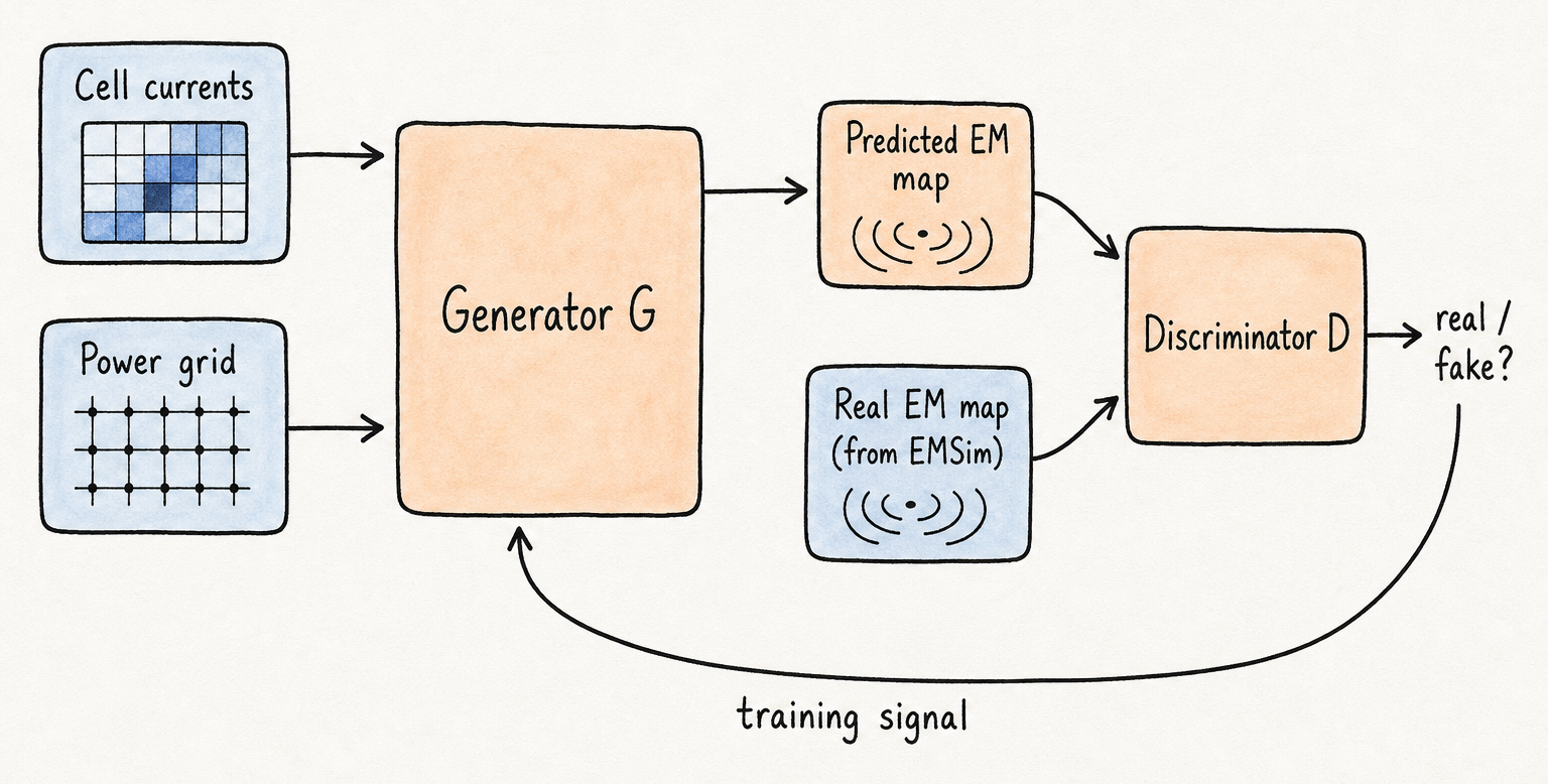
EMSim+ (ICCAD 2023) reframes simulation as a learning problem. The inputs to the learned model are the cell-current map per clock cycle and the design’s power-grid and clock-tree topology. The target output is the spatial EM emanation map at the chip surface — the same thing the physics simulator computes. If a learned model can reproduce those outputs accurately, inference replaces simulation, and the cost per trace drops to a single forward pass through the network.
The architecture we chose is a conditional generative adversarial network. A generator G takes the design inputs and produces a candidate EM map. A discriminator D takes either G’s output or a ground-truth EM map produced by EMSim on the same inputs and tries to tell them apart. The two are trained adversarially: G is pushed to produce maps that D cannot distinguish from real EMSim outputs; D is pushed to stay one step ahead. The conditioning on the input — the cell currents and grid topology — is what keeps the generator anchored to a specific design state rather than producing plausible-looking EM maps that correspond to no real computation.
The training objective formalizes this two-player game:
\[\min_{G}\max_{D} \; \mathbb{E}_{x,y}[\log D(x, y)] \;+\; \mathbb{E}_{x,z}[\log(1 - D(x, G(x, z)))]\]Read this as: G wins by producing EM maps the discriminator can’t tell apart from real EMSim outputs given the same inputs. Here $x$ is the conditioning input — the cell currents and power-grid structure — $y$ is the real EMSim-generated EM map for that input, and $z$ is a noise vector that lets the generator produce a distribution of plausible outputs rather than a single deterministic one. The conditioning on $x$ keeps the generator anchored to the actual design, not just a generic “EM map” distribution.
Training requires a dataset of (input, EMSim-ground-truth) pairs, which means paying EMSim’s physics cost once to generate that corpus. That is the right tradeoff: the training budget is amortized over every subsequent trace, and a design that needs 100K traces for evaluation will see the training cost paid back many times over by the end of the campaign. Once training is complete, inference is a forward pass — no differential equation solving, no sparse linear systems, no GPU-hours per trace.
On a 1M-trace evaluation campaign, EMSim+ reduced simulation time by 242× compared to EMSim. The benchmark set spanned Kyber, an AES processor extension, a masked AES core, and a 180 nm silicon AES-128. Accuracy against EMSim ground truth remained high, and attack predictions from EMSim+ traces matched silicon measurements at rates consistent with the physics simulator. The training cost — one-time, per design — was offset many times over once attack campaigns ran beyond a few thousand traces.
The 242× was real, but a GAN trained on one design only knew that one design — and design iteration is exactly when fast simulation matters most.
EMSim+ (GAN+TL) — generalization across designs
The 242× speedup from the GAN came with a cost that only appeared at the next design iteration. Training EMSim+ requires a ground-truth corpus of (input, EM map) pairs — and generating that corpus means running EMSim itself. For a single design evaluated once, that is an easy tradeoff: pay the physics cost once, amortize over millions of traces. For a design team iterating — modify the protection scheme, swap the countermeasure, migrate to a new process node — every change restarts the clock. The slow physics step runs again, then the training run, and fast simulation becomes available only after both finish. That is exactly the wrong moment for delay.
The deeper issue is that the ICCAD 2023 GAN learned a design-specific function. Its weights encoded how cell currents and power-grid topology in one particular layout mapped to EM maps at the chip surface. Those weights had nothing to say about other designs. Each new design was a cold-start problem.
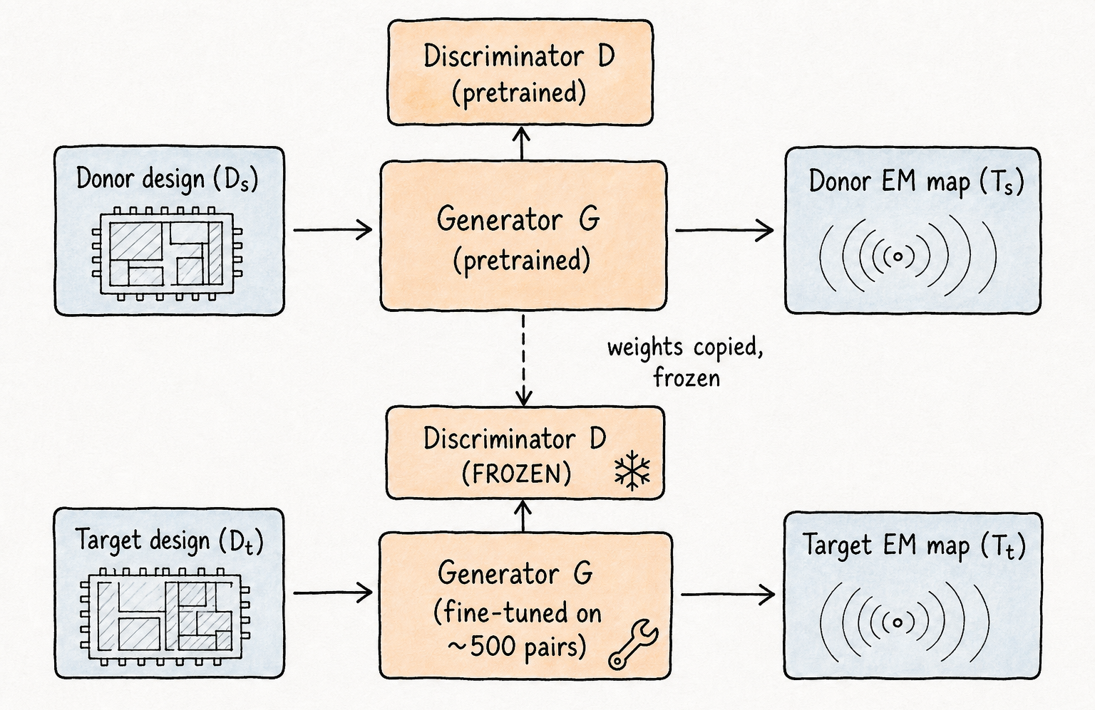
EMSim+ (GAN+TL), the TIFS 2024 extension, reframes this by asking what the GAN actually learns. The encoder in the generator does two conceptually different things. It learns general structure — the way current distributions in a layout give rise to surface EM fields, the role of power-grid density, the geometry of how switching events propagate through the interconnect. It also learns design-specific texture: the particular spatial pattern of this design’s clock tree, this design’s cell placement, this design’s power-grid routing. The general structure is largely the same across designs at the same technology node. Only the design-specific texture changes.
Transfer learning exploits this separation. We pretrain the full GAN on a donor design already simulated with EMSim — the AES baseline in our experiments. Once training converges, we freeze the discriminator: it has learned to distinguish real EM maps from generated ones, and that discriminative signal transfers. For a new target design, we fine-tune only the generator on a small EMSim corpus from that design. The discriminator stays frozen, providing a stable training signal; the generator adapts to the new design’s spatial patterns without abandoning the shared encoder features the pretraining established.
The training pipeline becomes: pretrain once on the donor design, freeze the discriminator, fine-tune the generator head on 500 sample pairs from the target design. The 500-pair figure is the headline result from the transfer learning experiments — compared to roughly 1,000 pairs needed for training from scratch, EMSim+ (GAN+TL) cuts the per-new-design EMSim burden in half, and the fine-tuning wall-clock time drops proportionally.
We evaluated this across five designs: the AES-128 baseline at 180 nm, two masked AES variants (AES_mask_1 with additive and multiplicative masking, AES_mask_2 with a cyclic-shift random mask scheme), AES_pg with physical power-grid protection strips, and AES_55nm — the same AES benchmark re-implemented in SMIC 55 nm CMOS. The last design is the hardest test: it is not just a logic change but a full technology-node migration, where parasitic profiles, cell geometries, and current signatures all shift. Across all five, the fine-tuned models achieved NCC and SSIM (structural similarity, the image-quality counterpart of NCC) exceeding 95%, matching the accuracy of models trained from scratch. Security evaluation by CEMA (correlation electromagnetic analysis, the EM analogue of CPA) on the fine-tuned traces correctly identified protected designs as resistant and flagged the unprotected baseline as leaky — consistent with silicon.
On the efficiency side, EMSim+ (GAN+TL) preserved the GAN’s throughput advantage. Against EMSim directly, it ran 113–149× faster per-dataset and 282–483× faster at the million-trace scale (the ranges span the five evaluated designs; the 242× headline from the prior section is for the single AES-128 baseline). The added benefit of transfer learning was not speed per trace — inference cost is the same whether weights came from pretraining or from scratch — but the reduction in the upfront cost required before any inference could happen. Pretraining amortizes across every subsequent design. Fine-tuning on 500 pairs is a fraction of a day’s EMSim compute. The fast-simulation capability now became available for a new design almost immediately, which is the property that matters in a real iteration loop.
Across the EMSim → EMSim+ → EMSim+ (GAN+TL) lineage, every step bought speed or generalization on the EM channel. The next problem was about a different channel entirely.
AIPS — diffusion for power, not just EM
The EMSim and EMSim+ lineage closed Problems 1, 2, and 3 — but all three solutions were built around the EM channel. Power is the SCA channel with the deeper literature, the broader attacker community, and the simpler measurement setup: a current probe on the supply rail beats a near-field EM probe in portability and repeatability. Any design evaluation framework that stops at EM is, at minimum, incomplete.
There is also a tool gap on the power side that doesn’t exist in the same way on the EM side. Synopsys PrimeTime PX (PTPX) is the de-facto vendor reference for transient power simulation in digital design flows. It is accurate, well-validated against silicon, and the result most design teams trust when they need ground truth. It is also the slowest step in any modern pre-silicon SCA evaluation: PTPX is built to answer thermal and voltage-variation questions, where average power per clock cycle is the quantity of interest. SCA attacks are different. They exploit nanosecond-scale transient waveforms — the momentary current spikes that encode data-dependent switching activity across individual logic paths — not long-window averages. Existing AI-based power-estimation tools developed for thermal-aware floorplanning and IR-drop analysis operate in that average-power regime. They are fast and useful, but their outputs lack the fine-grained temporal structure that correlation power analysis actually attacks. The gap: fast, accurate, nanosecond-resolution transient power simulation for pre-silicon SCA evaluation.
AIPS (TCHES 2026) is our answer to Problem 4. It crosses two boundaries at once: from the EM channel to the power channel, and from the GAN architecture we used in EMSim+ to a diffusion model as the generative backbone. The choice to revisit the architecture was deliberate, and it matters for why AIPS generalizes to the breadth of designs we evaluated.
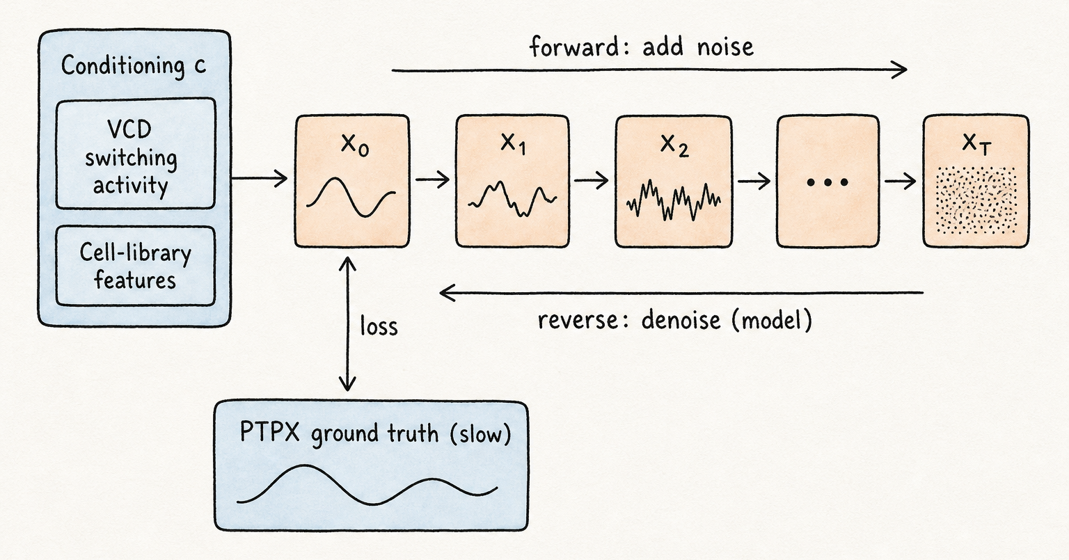
Training data for AIPS is a corpus of power traces produced by PTPX — the slow, accurate ground truth. The conditioning signal that tells the model what is happening in the chip is constructed from two sources: the per-cycle switching activity extracted from the design’s VCD (value change dump), which records which cells change state at each clock edge; and technology-library features capturing the timing and power characteristics of each cell type in the standard-cell library. Together these describe what the chip is computing, cycle by cycle, in terms the model can learn to map to a transient power waveform. The output is a time-series trace of arbitrary length at nanosecond resolution — the same format PTPX would produce, but generated at inference cost rather than simulation cost.
The shift from GAN to diffusion is not incidental. A GAN learns to fool a discriminator; its training signal is adversarial, which gives excellent average-case quality but can produce mode collapse — the generator settling into a narrow band of outputs that satisfy the discriminator while failing to cover the full distribution of traces a real chip would produce. For SCA evaluation, mode collapse is dangerous: if the synthetic traces all look similar, a statistical attack campaign loses the trace diversity it needs to average out noise and reach reliable conclusions. Diffusion models learn to denoise gradually: they are trained to reverse a forward process that adds Gaussian noise to a trace over many steps, and at inference time they run that reverse process from pure noise to a clean trace. That formulation naturally supports diverse outputs — different noise seeds produce statistically independent traces — while the conditioning keeps each output anchored to the workload.
The conditional reverse-diffusion step is:
\[p_\theta(\mathbf{x}_{t-1} \mid \mathbf{x}_t, \mathbf{c}) \;=\; \mathcal{N}\!\left(\boldsymbol{\mu}_\theta(\mathbf{x}_t, t, \mathbf{c}),\; \boldsymbol{\Sigma}_\theta(\mathbf{x}_t, t, \mathbf{c})\right)\]Read this as: at every denoising step, the model predicts a Gaussian over the cleaner trace, conditioned on the workload $\mathbf{c}$. Run the chain $T$ steps and you have a synthetic transient that matches PTPX in distribution. New noise seed → new trace; same $\mathbf{c}$ → same workload; consistent statistics across an arbitrarily large attack campaign.
The efficiency picture separates into two modes. At inference time — after training is complete — generating a trace requires only the forward pass through the diffusion sampler: new noise seed in, new trace out, no PTPX invocation. That inference-only mode delivers the largest absolute speedup. Even with the full training cost amortized in, the framework wins at the 100K–1M-trace scale that SCA campaigns actually run — the concrete numbers below quantify that.
We evaluated AIPS on five targets chosen to span the realistic scope of what a design team might need to evaluate:
- AES (the baseline cipher, unmasked)
- Kyber (a NIST-selected post-quantum key-encapsulation mechanism)
- Two masked AES variants (testing higher-order SCA, where countermeasures actively complicate leakage)
- A RISC-V core (a general-purpose processor executing AES, not a dedicated crypto block)
Across all five, AIPS traces matched PTPX ground truth under waveform-similarity metrics and reproduced the same SCA evaluation outcomes — the same key-recovery results under first-order attacks, and the same higher-order leakage assessments where masking was present. On efficiency:
- 4–42× faster than PTPX at 1M traces (training cost included; precise figures in the comparison table below)
- Up to 10⁴× per-trace speedup once training is amortized
- ~1K training traces sufficient for full accuracy — a corpus PTPX can produce in tractable time
- Throughput advantage compounds with trace length
Across four papers, every step bought a different axis of capability. The next section reads them as a single design space.
What changed across the lineage
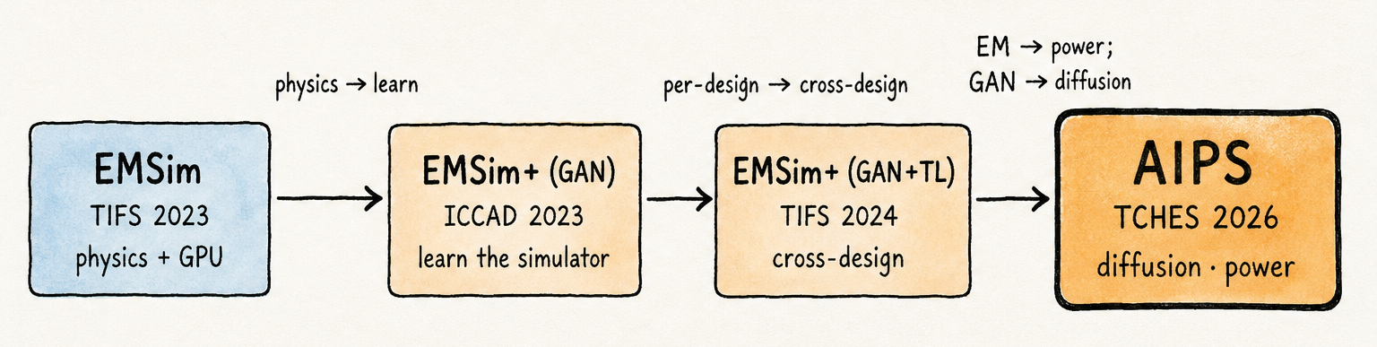
Laid out as a single diagram, the lineage reveals something no individual paper states: every step bought a different axis of capability, and every step’s inherent limitation was exactly what motivated the next.
The first transition — physics to learn — moved the throughput ceiling by an order of magnitude by trading per-trace simulation cost for an upfront training corpus.
The second transition — per-design to cross-design — reduced the activation cost of that learned simulator to a fine-tuning run on a few hundred pairs, making fast simulation available at the start of a design iteration rather than at the end.
The third transition — EM to power, with the backbone shifting from GAN to diffusion at the same step — opened a second channel and replaced an adversarial training objective with one that naturally supports the trace diversity that power-side SCA evaluation demands.
Reading the steps together: speed, generality, breadth — each gained one axis, each left the next axis to the following paper.
| Paper | Channel | Backbone | Generalization | Training data | Speedup vs. ground truth | Validated on |
|---|---|---|---|---|---|---|
| EMSim | EM | physics + parasitic reduction + GPU | per design | n/a | 32× over baseline | S-Box, AES (SMIC 180 nm silicon) |
| EMSim+ (GAN) | EM | conditional GAN | per design | ~1K pairs (per design) | 242× over EMSim at 1M traces | Kyber + 3 AES variants (extension, masked, 180 nm silicon) |
| EMSim+ (GAN+TL) | EM | GAN + transfer learning | cross-design + cross-node | ~500 fine-tune pairs | 113–149× per-dataset; 282–483× at 1M-trace scale | 5 designs, 180 nm + 55 nm |
| AIPS | Power | conditional diffusion | multi-target (5 designs) | ~1K traces | 4.14–42.44× over PTPX; up to 10⁴× inference-only | AES, Kyber, masked AES (×2), RISC-V |
The structure of the lineage matters because it rules out a simpler reading. These are not four attempts at the same problem, each a bit faster. EMSim answered: can physics-accurate EM simulation run at evaluation scale? EMSim+ (GAN) answered: can a learned model replace per-trace physics simulation? EMSim+ (GAN+TL) answered: can that learned model be reused across designs without starting over? AIPS answered: can a different generative architecture extend the approach to the power channel while preserving the trace diversity that channel demands? Each question was only visible because the previous answer made it concrete. The lineage is a sequence of specific bottlenecks resolved in sequence, not a progression toward a single target efficiency number.
That is the post’s central claim, stated plainly: pre-silicon SCA evaluation isn’t one problem but a family of them.
Open problems
Masked and post-quantum (PQC) designs at scale. AIPS already evaluates Kyber and two masked AES variants, but higher-order masking — third-order and beyond — and larger post-quantum cryptography (PQC) schemes such as Dilithium-style signatures, Falcon, and full hybrid TLS stacks place different demands on any simulation framework. Rare leakage events become rarer, training-data requirements grow with design complexity, and the SoC context surrounding a crypto core introduces switching activity that a crypto-block-only evaluation can miss. Diffusion’s per-trace cost matters more as design scope expands, not less — campaign sizes grow with the design, so any regression in throughput compounds.
Closing the loop with countermeasure synthesis. Evaluation tells you where leakage exists; protection tells you how to fix it. Identifying a leaky net or path in simulation is only useful if there is a way to act on that information without re-running the full evaluation cycle after every candidate fix. PathFinder (DAC 2022 · PDF) and Formal Path (TECS 2025 · PDF) — our work on automatic leaky-path identification and logic-level obfuscation — are our take on the protection side of this loop. A future post will cover them in the same depth as the evaluation lineage covered here.
Code
-
github.com/jinyier/EMSim— EMSim and EMSim+ implementations. -
github.com/jinyier/AIPS— AIPS implementation.
References
- H. Ma, M. Panoff, J. He, Y. Zhao, Y. Jin. EMSim: A Fast Layout Level Electromagnetic Emanation Simulation Framework for High Accuracy Pre-Silicon Verification. IEEE Transactions on Information Forensics and Security, 2023. PDF
- Y. Gao, H. Ma, J. Kong, J. He, Y. Zhao, Y. Jin. EMSim+: Accelerating Electromagnetic Security Evaluation with Generative Adversarial Network. IEEE/ACM ICCAD, 2023. PDF
- Y. Gao, H. Ma, Q. Zhang, X. Song, Y. Jin, J. He, Y. Zhao. EMSim+: Accelerating Electromagnetic Security Evaluation With Generative Adversarial Network and Transfer Learning. IEEE Transactions on Information Forensics and Security, 2024. PDF
- Y. Gao, H. Ma, T. Zhang, J. He, Y. Zhao, M. Stojilović, Y. Jin. AIPS: AI-Based Power Simulation for Pre-Silicon Side-Channel Security Evaluation. IACR Transactions on Cryptographic Hardware and Embedded Systems, 2026. PDF
- H. Ma. Research on Pre-Silicon Security Evaluation and Protection Techniques for Cryptographic Chip. Ph.D. Thesis, Tianjin University, 2023. PDF